- Details
- Written by Administrator
- Category: Uncategorised
- Hits: 2291
https://www.shizuoka.ac.jp/english/
http://ems.eng.shizuoka.ac.jp/english/
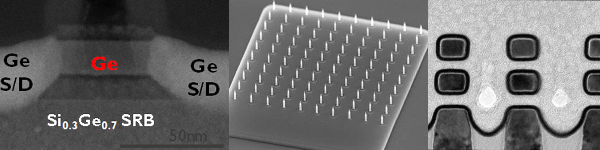
Attention to implementation of Group-IV alloys including SiGe, GeSn, SiGeSn, etc. into Thermoelectric (TE) devices is getting increased. Alloy effect effectively decreases heat propagation in a material, resulting in improvement of conversion efficiency of TE devices. Our groups are developing the growth technique of these alloys especially on insulator substrates and investigating the impact of crystallographic properties on TE conversion efficiency.
Ikeda laboratory https://wwp.shizuoka.ac.jp/ikedalab-en/
- Polycrystalline SiGe on insulator (SGOI)
- Si nanowire (NW)
Shimura laboratory
https://tdb.shizuoka.ac.jp/RDB/public/Default2.aspx?id=11200&l=1
- Polycrystalline GeSn and Si-rich SiGeSn on insulator
- Sn-nanodot mediated solid-phase crystallization
- Details
- Written by Administrator
- Category: Uncategorised
- Hits: 2787
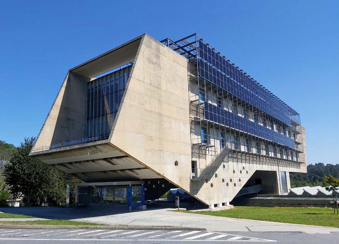
The New Materials group FA3 of the Applied Physics Department at the University of Vigo is member of the Research Center in Technologies, Energy and Industrial Processing (CINTECX) and of the Southern Galicia Institute of Health Research (IISGALICIASUR).
The groups R&D activities are based on UV-laser processing of semiconductors and biomaterials, and development of 2-D materials, chiroptical structures, 3-D printed scaffolds, characterization of surfaces, interfaces and thin films, and on the"in-vitro" behaviour of living cells for tissue engineering.
Its mission is the transfer of results and technologies to both, scientific community and market for applications in biomedicine, bioengineering, photonics, microelectronics, and nanotechnology.
Contact: Dr. Stefano Chiussi
Facebook: @NewMaterialsGroup, Web: http://cintecx.uvigo.es/![]()
Address: New Materials Group, E. E. Industrial -Campus Universitario, E-36310 Vigo (Spain)
 Processing and characterization of thin films and heterostructures based on all group-IV elements is one of its main specific research areas.
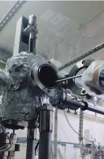
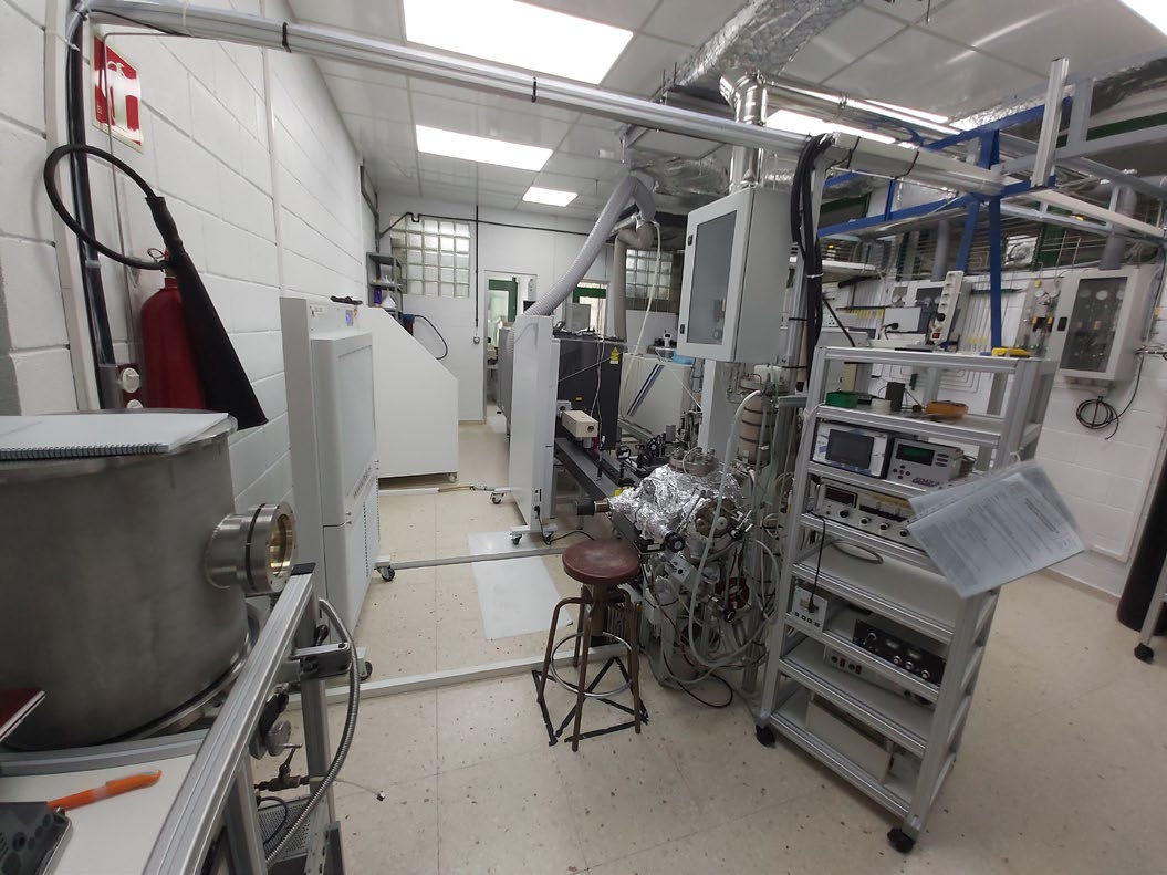
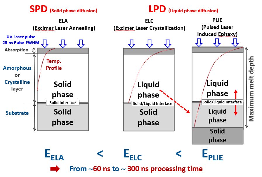
Material processing activities are performed in a certified 40 m2 ISO-7 Cleanroom with ISO-6 laser processing areas and focused on 193 nm Laser CVD of Boron doped and intrinsic amorphous SiGeC alloys, PVD and PLD of thin Sn, Pb films and193 nm Laser assisted annealing (ELA) crystallization (ELC) and epitaxy (PLIE).
PVD and 193 nm laser processing areas
The aim of studying these 193 nm laser assisted techniques is to control, in thin films and heterostructures with group IV elements (C, Si, Ge, Sn, Pb) and alloys, processes such as impurity doping and dopant activation, formation of nanocrystalline heterostuctures on flexible polymer surfaces, and of epitaxial SiGe, SiGeSn and GePb alloys on virtual Ge substrates. Key target in epitaxy studies is to tailor the local (lateral and in depth) temperature profiles of the 25 ns short homogenized 193 nm laser pulses and evaluate its effects on fast melting and solidification processes. The infrastructure for characterization of group.-IV materials includes AFM-Raman (4 wavelength), XPS, TOF-SIMS, HFIB, HR-TEM/STEM, FTIR and SE.
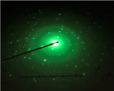
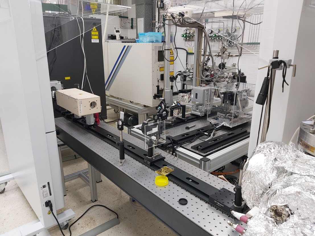
Example v-Ge coated with Sn and irradiated with 193 nm pulses trough a homogenizer and a mask projection unit:
193 nm Laser processing fundamentals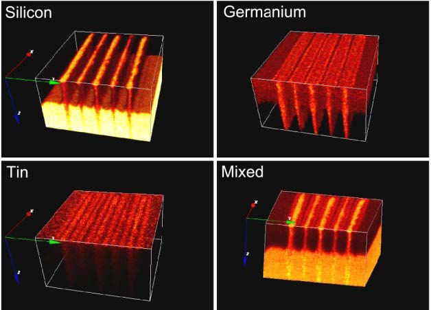
3-D TOF-SIMS images of element distribution in a line pattern obtained with 10 laser pulses.
(a) CM image of a line section, (b) TEM image of a line border, (c) AFM-Raman scan of a line border with pure Ge peak outside and SiGeSn peaks in the line. SiGeSn spectrum from the line center at the bottom of the image.
External funding in the last years (2017-2020):
*Sistemas Moleculares y Supramoleculares para Transducción Sensórica (SMol-Supra-Sens), Ministerio de Economía y Competitividad CTQ2014-58629-R, 2014-2017, 83 000 €
*Sistemas Quirópticos, Chiropticalsystems (Chiroptic-S), Ministerio de Economía y Competitividad, ”Redes de Excelencia CTQ2015-71924-REDT”, 2015-2017, 25 000 €
*Instituto de Bioingeniería en Red para el Envejecimiento Saludable (IBEROS), EU Fondo europeo de desarrollo Regional (POCTEP) (0245_IBEROS_1_E), 2017-2019, 1 463 958 €
*Inovaçao industrial atravésde colaboracaos especificas entre empresas e centros de investigaçao no contexto de valorizaçao biotecnológica marinha (CVMar+i), EU Fondo europeo de desarrollo Regional (POCTEP) (0302_CVMAR_1_1_P), 2017-2019, 2 230 496 €
*Consolidación y estructuración de unidades de investigación competitivas Modalidad grupos de referencia competitiva: “Grupo FA3 Novos Materiais”, Xunta de Galicia ED431C 2017/51, 2017-2020, 200 000 €
*Consolidación y estructuración de unidades de investigación competitivas Modalidad Redes: “Rede Galega de Biomateriais”, Xunta de Galicia GRR2014/033, 2017-2019, 120 000 €
*Biomaterial para regeneración ósea (BIOFAST) Programa IgniciaProba de Concepto (Gain-Xunta de Galicia), 2017-2019, 247 120 €
*CARIOSCOPE, EU POCTEC-Código Máis, 2018 -2018, 37 500 €
*BLUE biotechnology as a road for innovation on HUMAN’s health aiming smart growth in Atlantic Area (BLUEHUMAN), EU Programa Interreg ATLANTIC AREA, 2018-2020, 150 537 €
*BLUBIOLAB –“Laboratorio Transfronterizo de Biotecnología Marina”, EU Programa de Cooperación InterregV (POCTEP 2014-2020) 2019 –2022, 272 651 €
Most relevant publications in the last years (2015-2020) (* Related to biomedicine, tissue engineering and chiroptics, ** related to Group IV)
** S. Wirths et al. Lasing in direct bandgap GeSn alloy grown on Si (001), Nature Photonics (2015) 9(2) 88-92 https://doi.org/10.1038/nphoton.2014.321
**F. Oliveira et al. Multi-stacks of epitaxial GeSn self-assembled dots in Si: Structural analysis, Journal of Applied Physics (2015) 117 (12), https://doi.org/10.1063/1.491593
** I.A. Fischer et al. Growth and characterization of SiGeSn quantum well photodiodes, OpticsExpress (2015) 23 (19) 25048, https://doi.org/10.1364/OE.23.025048
**F. Oliveira et al. Fabrication of GeSn-multiple quantum wells by overgrowth of Sn on Ge by using molecular beam epitaxy, Applied Physics Letters (2015) 107 (26), https://doi.org/10.1063/1.4938746
** F. Gontad et al. 193 nm Excimer laser processing of Si/Ge/Si(100) micropatterns, Applied Surface Science (2016) 362, 217-220, https://doi.org/10.1016/j.apsusc.2015.11.240
**T. Wendav et al. Photoluminescence from ultrathin Ge-rich multiple quantum wells observed up to room temperature: Experiments and modeling, Physical review B –Condensed Matter and Materials Physics (2016) 94(24), https://doi.org/10.1103/PhysRevB.94.245304
**I. A. Fischer et al. (Si)GeSn nanostructures for optoelectronic device applications, IEEE Proceedings MIPRO (2016) 1-4, DOI: 10.1109/MIPRO.2016.7522099, Electronic ISBN:978-953-233-086-1
*R. Valdés et al. Ex vivo analysis of the oral epithelium by high-wavenumber Raman spectroscopy, International Journal of Biomedical Engineering and Technology (2017) 24(2) 154-168, https://dx.doi.org/10.1504/IJBET.2017.084665
** J. Schlipf et al. Growth of patterned GeSn and GePb alloys by pulsed laser induced epitaxy, IEEE Proceedings MIPRO (2017) 37-42 https://doi.org/10.23919/MIPRO.2017.7973387
*H. Aguiar et al. Structural characterization of bio ceramics and mineralized tissues based on Raman and XRD techniques Ceramics International (2018) 44(1) 495-504, https://doi.org/10.1016/j.ceramint.2017.09.203
* A.Ozcelik et al. Device-Compatible Chiroptical Surfaces through Self-Assembly of Enantiopure Allenes, Langmuir 2018) 34(15) 4548-4553 https://pubs.acs.org/doi/abs/10.1021/acs.langmuir.8b00305
*M. López-Álvarez et al, Osteogenic effects of simvastatin-loaded mesoporous titania thin films, Biomed Mater.13 (2018) 025017 https://doi.org/10.1088/1748-605X/aa95f1
*M. López-Álvarez et al. Quantitative evaluation of sulfation position prevalence in chondroitin sulphate by Raman spectroscopy, Journal of Raman Spectroscopy 50 (2019) 656-664 https://doi.org/10.1002/jrs.5563
** M.C.J.Weiser et al. Fabrication of GePb-Alloys by Means of Pulsed Laser Induced Epitaxy, IEEE Proceedings MIPRO (2019) 1-6,, DOI: 10.23919/MIPRO.2019.8756640, ISSN: 2623-8764
** J.Schlipf et al. Ellipsometric analysis of concentration gradients induced in semiconductor crystals by pulsed laser induced epitaxy, J. of Vacuum Science and Technology B: Nanotechnology and Microelectronics B 37, 061213 (2020) (2019) 1-6, https://doi.org/10.1116/1.5122777¨
- Details
- Written by Administrator
- Category: Uncategorised
- Hits: 3917
Short description of activities
The research activities within Group IV semiconductors mainly concentrate on process technology optimization for reliable silicon, silicon carbide (SiC) and Carbone based devices. The devices are fabricated in our IMB-CNM Clean Room and they are intended for various application fields (energy, mobility, high frequency, harsh environment, space applications, high energy physics experiments, etc.). The research studies cover the simulation, design, fabrication and characterization of a wide range of structures (Schottky diodes, bipolar diodes, MOS capacitances, MESFETs, MOSFETs, JFETs, etc…), as well as their integration in basic ICs.
1. Optimized process technologies for wide bandgap semiconductors: silicon carbide (SiC), gallium nitride on silicon (GaN on Si) and more recently diamond.
Some of the main issues addressed in SiC and GaN technology cover from junction and contact formation to optimization of gate oxidation process, with research on different approaches to improve the gate dielectric and its interface with the semiconductor (Rapid Thermal Processing, TEOS PECVD, nitridation, high-k dielectrics, etc…), as well as other treatments, like boron-doped gate dielectrics for high channel mobility SiC MOSFETs.
An important part of the activities concentrates also on dedicated electrical characterization and reliability assessment techniques of the involved WBG technologies, including for example characterization at different temperatures, bias-stress instability and radiation hardness stability studies.
2. Fabrication of high-temperature devices (diodes, sensors, integrated circuits) for aeronautical and space applications.
Taking profit of the available advanced technology, SiC devices for sensors applications (Hall sensors, Gas sensors, UV detectors, Biomedical sensors, NEMS, etc...) are also a matter of research, some of them in collaboration with other multidisciplinary Groups. We have also developed digital electronic gates and basic circuits like flip-flop for high temperature (300ºC) integrated circuits. We are currently working on high temperature SiC CMOS structures, as well as on the development of wide temperature range (-40ºC-300ºC) voltage references.
3. Study of carbon-based materials
Another relevant activity is toward the study and technology integration of carbon-based materials as, for example, epitaxial graphene on SiC or CVD graphene, carbon nanotubes and, more recently, diamond devices. Processing technologies for the implementation of Carbone based devices are under development and several devices demonstrators have been successfully obtained. Applications in different fields like quantum technology, metrology, biosensors are contemplated.
These activities have been developed in the framework of different National and International Research Projects and Industrial contracts, as for example:
• Green Electronics with Diamond Power Devices (GreenDiamond), H2020-LCE-2014-1, Grant agreement ID: 640947, May 2015 – Apr. 2020
• Silicon Carbide Power Technology for Energy Efficient Devices (SPEED), FP7-NMP-2013-LARGE-7, Grant agreement ID: 604057, Jan. 2014 - Dec. 2018
• Current Limiting Device to Address DC Aeronautics Power Distribution Systems (FUSES 2014), SP1-JTI-CS-2013-03, Grant agreement ID: 641336, 1 Sep 2014 – 31 Aug 2016
• Prototyping and characterisation of radiation hardness of SiC MOS structures
European Space Agency: 01ITT AO/16962/12/NL/SFe, 1 july 2015 – 31 may 2018
• Training NETwork on Functional Interfaces for SiC (NETFISIC), FP7-PEOPLE-2010-ITN, Grant agreement ID: 264613, 1 Feb 2011 – 31 Jan 2015
• Development of a high voltage Silicon Carbide (SiC) normally–on JFET with vertical conduction architecture for cascode applications
Industrial contract with Monolithic Power Systems (US) 01/06/2018 - 31/09/2020
• Fabrication of epitaxial graphene on silicon carbide
Industrial contract with Graphene Nanotech (Spain
For more details, please visit our web page: http://www.imb-cnm.csic.es/index.php/en/
Contact:
|
Prof. Philippe Godignon |
Email: This email address is being protected from spambots. You need JavaScript enabled to view it. |
|
Dr. Joan Marc Rafí |
Email: This email address is being protected from spambots. You need JavaScript enabled to view it. |
Selected representative publications (2015-2020)
2020:
J.M. Rafí, G. Pellegrini, P. Godignon, et al., Electron, neutron and proton irradiation effects on SiC radiation detectors, IEEE Transactions on Nuclear Science 67 (12), 2481-2489 (2020), https://doi.org/10.1109/TNS.2020.3029730
M.C. Jiménez-Ramos, et al., IBIC analysis of SiC detectors developed for fusion applications, Radiation Physics and Chemistry 177, 109100 (2020), https://doi.org/10.1016/j.radphyschem.2020.109100
J.C. Hönig, et al., Investigation of nitrogen enriched silicon for particle detectors, Journal of Instrumentation 15, P05006 (2020), https://doi.org/10.1088/1748-0221/15/05/P05006
S. Aslanidou, A.García-García, P. Godignon, G. Rius, Electronic interface and charge carrier density in epitaxial graphene on silicon carbide. A review on metal–graphene contacts and electrical gating, APL Materials 8, 100702 (2020), https://doi.org/10.1063/5.0022341
2019:
M. Cabello, et al., Comparative study of boron doped gate oxide impact on 4H and 6H-SiC n-MOSFETs, Materials Science in Semiconductor Processing 93, 357-359 (2019), https://www.sciencedirect.com/science/article/pii/S1369800118319309
E. Masvidal-Codina, et al., High-resolution mapping of infraslow cortical brain activity enabled by graphene microtransistors, Nature Materials 18, 280-299 (2019), https://www.nature.com/articles/s41563-018-0249-4
V. Banu, M. Popescu, P. Godignon, Delta Reference, the Latest High Temperature Compensated Voltage Reference Concept, European Space Power Conference (ESPC) Juan-les-Pins, FRANCE SEP 30-OCT 04, 2019
2018:
V. Soler, M. Cabello, V. Banu, J. Montserrat, J. Rebollo and P. Godignon, Complementary p-Channel and n-Channel SiC MOSFETs for CMOS Integration, Material Science Forum, vol. 924, pp.975-979 (2018)
O. Loto, et al., Gate Oxide Electrical Stability of p-type Diamond MOS Capacitors, IEEE Transactions on Electron Devices 65, 3361-3364 (2018), https://ieeexplore.ieee.org/document/8399540
M. Cabello, et al., Advanced processing for mobility improvement in 4H-SiC MOSFETs: A review, Materials Science in Semiconductor Processing 78, 22-31 (2018), https://www.sciencedirect.com/science/article/pii/S1369800117318978
F. Roccaforte and P. Godignon, Wide band gap semiconductors technology for next generation of energy efficient power electronics, Editorial of Special Issue Materials Science in Semiconductor Processing 78, 1-1 (2018), https://www.sciencedirect.com/science/article/pii/S136980011830101X
C. Hebert, et al., Flexible Graphene Solution-Gated Field-Effect Transistors: Efficient Transducers for Micro-Electrocorticography, Advanced Functional Materials 28, 1703976, (2018), https://onlinelibrary.wiley.com/doi/full/10.1002/adfm.201703976
J.M. Rafí, et al., Four-quadrant silicon and silicon carbide photodiodes for beam position monitor applications: electrical characterization and electron irradiation effects, Journal of Instrumentation 13, C01045, (2018), https://iopscience.iop.org/article/10.1088/1748-0221/13/01/C01045
2017:
V. Soler, et al., High-Voltage 4H-SiC Power MOSFETs With Boron-Doped Gate Oxide, IEEE Transactions on Industrial Electronics 64, 8962-8970 (2017), https://ieeexplore.ieee.org/document/7968463
J.C. Pinero, et al., Impact of Thermal Treatments in Crystalline Reconstruction and Electrical Properties of Diamond Ohmic Contacts Created by Boron Ion Implantation, Physica Status Solidi A 214, 1700230 (2017), https://onlinelibrary.wiley.com/doi/full/10.1002/pssa.201700230
M. Cabello, et al., Impact of boron diffusion on oxynitrided gate oxides in 4H-SiC metal-oxide-semiconductor field-effect transistors, Applied Physics Letters 111, 042104 (2017), https://aip.scitation.org/doi/10.1063/1.4996365
2016:
V. Banu, et al., Power cycling analysis method for high-voltage SiC diodes, Microelectronics Reliability 64, 429-433 (2016), https://www.sciencedirect.com/science/article/pii/S0026271416301913
2015:
M. Alexandru, et al., SiC Integrated Circuit Control Electronics for High-Temperature Operation, IEEE Transactions on Industrial Electronics 62, 3182-3191 (2015), https://ieeexplore.ieee.org/document/6982217
J. Leon, et al., Local non invasive study of SiC diodes with abnormal electrical behavior, Solid-State Electronics 113, 35-41 (2015), https://www.sciencedirect.com/science/article/pii/S0038110115001409
T. Phulpin, et al., Failure analysis of ESD-stressed SiC MESFET, Microelectronics Reliability 55, 1542-1548 (2015), https://www.sciencedirect.com/science/article/pii/S0026271415300585
G. Pristavu, et al., A model to non-uniform Ni Schottky contact on SiC annealed at elevated temperatures, Applied Physics Letters 106, 261605 (2015), https://aip.scitation.org/doi/10.1063/1.4923468
V. Banu, P. Godignon, J. Millan, Design of Voltage Comparator Integrated Circuit with Normally-On MESFETs on 4H-SiC semiconductor, IEEE International Semiconductor Conference Sinaia (Romania) OCT 12-14, 2015
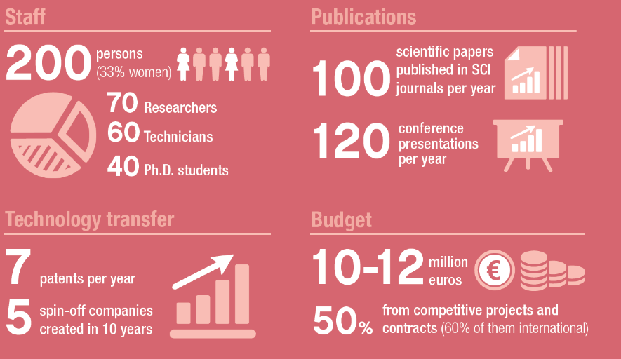
Short description of IMB-CNM-CSIC
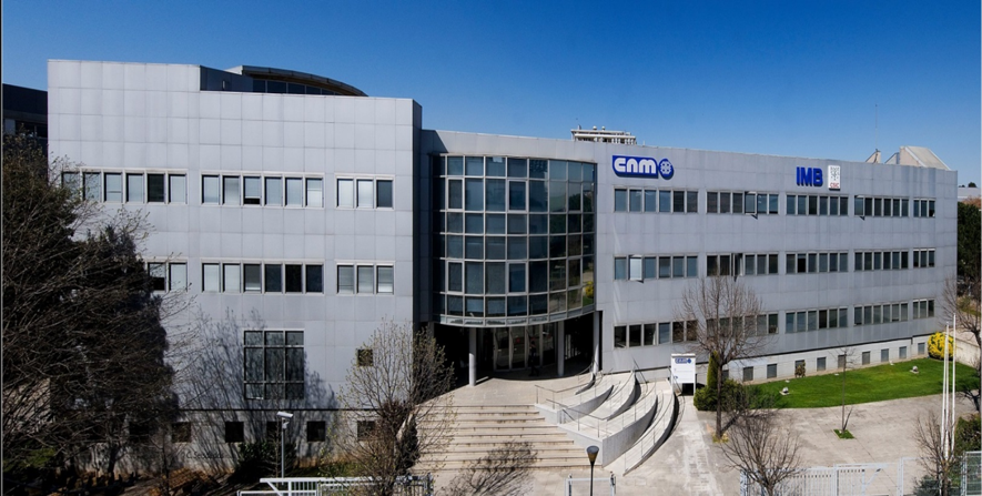
The Institute of Microelectronics of Barcelona (IMB-CNM) is the largest institute in Spain dedicated to the research and development of Micro and Nano Technology (MNTs) and microsystems and the unique with the capacities of silicon technology in Spain. It belongs to the Spanish National Research Council (CSIC) since its foundation in 1985
IMB-CNM is located in Bellaterra (Cerdanyola del Vallès), on the Campus of the Autonomous University of Barcelona (UAB), which is a privileged environment for both basic and applied/industrial research. It is a member of the Barcelona Nanotecnology Cluster-Bellaterra. The IMB-CNM as part of CSIC is also a member of the UAB Research Parc (PRUAB).
IMB-CNM mission is to perform applied research based on micro and nanotechnologies, mainly focused towards the development of components and micro and nano systems. IMB-CNM aims to contribute to the advancement of knowledge and to the economic and social development of society, as well as to the training of researchers and engineers and to the advice to public and private entities.
Intelligent miniaturized systems, eventually with integrated electronic, photonic, mechanical components and circuits, play an important role in society. Research, development and application of miniaturized components and systems will improve the health and well-being of people, help control environmental conditions, save and improve efficient management of energy. IMB-CNM aims to be a recognized contributor in exploring and developing micro and nanotechnologies for the realization of miniaturized components and systems. Its experience in micro and nanotechnologies enables IMB-CNM to lead projects ranging from academic research to industrial contracts, in an international environment.
The R&D activities of IMB-CNM are complemented with training of students, researchers and engineers and with technology transfer to companies.
IMB-CNM also participates in Spanish and International Technology Platforms and Networks of Excellence and has established collaborative agreements with various universities and research centres, to which it offers cooperation in their R&D activities and also access to manufacturing technologies through the "Integrated Micro and Nanofabrication Clean Room". This infrastructure has been recognized by the Ministry of Economy and Competitiveness with the National label of large-scale infrastructure (Instalación Científica y Tecnológica Singular - ICTS).

IMB-CNM summary
- Details
- Written by Administrator
- Category: Uncategorised
- Hits: 2513
Kyushu University
The advanced functional devices division, Global Innovation Center (GIC), Kyushu University focuses on research about group IV semiconductors (Si, Ge) 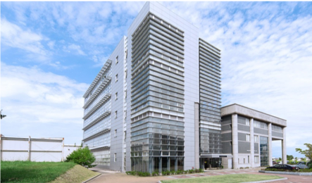 including their alloy (SiGe, GeSn) and compounds (SiC) process technology and characterization. We promote collaborative study with academic sections and industries all over the world.
Website: https://www.gic.kyushu-u.ac.jp/functionaldevices/index_e.htm
Contacts: Assist Prof. Keisuke YAMAMOTO
Recently we focus on the following topics:
- Ge process technology for MOSFET, optoelectronics, spintronics, and tunnel FET
Ge gate stack
Metal/Ge contact
Ge-on-Insulator
- Polycrystalline Ge, GeSn growth and device fabrication
- Defect characterization in Ge, Ge MOS
- 3C-SiC process technology
Process equipment
Cleanroom (class 1000, 200 m2), ECR sputtering system,
ALD, PVD (sputtering, EB evaporation), electric furnace, RTA, photolithography environment, RIE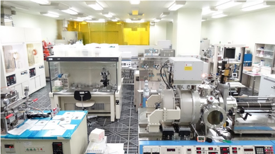
Evaluation equipment
DLTS, Hall effect, C-V/I-V measurements, MOSFET measurements, μ-raman/Photoluminescence, AFM, SEM/TEM (in the same campus), XPS (in the same campus)
Collaborations
Osaka Univ., Japan (Prof. HAMAYA (spintronics))
Tokyo City Univ., Japan (Prof. SAWANO (IV-MBE))
Tsukuba Univ., Japan (Assoc. Prof. TOKO (thin polycrystalline)) Nagoya Univ., Japan (Prof. Nakatsuka)
imec, Belgium
Shanghai Institute of Microsystem and Information Technology, Chinese Academy of Science (Prof. DI)
Recent publications
- K. Yamamoto et al., Fabrication of Ge-on-Insulator By Epitaxial Growth and Ion-Implanted Exfoliation for Electronics and Opt-Electronics Applications, ECS transactions, in press (2021).
- K. Yamamoto et al., Schottky Barrier Height Control at Metal/Ge Interface by Insertion of Nitrogen Contained Amorphous Layer, ECS transactions Vol. 102, No. 4, p. 63 (2021), https://doi.org/10.1149/10204.0063ecst
- H. Nakashima et al., Border-Trap Characterization for Ge Gate Stacks with Thin GeOX layer Using Deep-Level Transient Spectroscopy, ECS transactions, Vol. 98, No. 5, p. 395 (2020), https://doi.org/10.1149/09805.0395ecst
- W.-C. Wen et al., Interface trap and border trap characterization for Al2O3/GeOx/Ge gate stacks and influence of these traps on mobility of Ge p-MOSFET, AIP advances, in press, https://doi.org/10.1063/5.0002100
- R. Oka et al., High interfacial quality metal-oxide-semiconductor capacitor on (111) oriented 3C-SiC with Al2O3 interlayer and its internal charge analysis, Jpn. J. Appl. Phys., Vol. 59, p. SGGD17 (2020), https://doi.org/10.35848/1347-4065/ab6862
- K. Yamamoto et al., Conduction Type Control of Ge-on-Insulator: Combination of Smart-CutTM and Defect Elimination, ECS transactions, Vol. 93, No. 1, p. 73(2019) https://dx.doi.org/10.1149/09301.0073ecst
- K. Moto et al., Polycrystalline thin-film transistors fabricated on high-mobility solid-phase-crystallized Ge on glass, Appl. Phys. Lett., Vol. 114, p. 212107 (2019), https://doi.org/10.1063/1.5093952
- K. Yamamoto et al., Ge field-effect transistor with asymmetric metal source/drain fabricated on Ge-on-Insulator: Schottky tunneling source mode operation and conventional mode operation, Jpn. J. Appl. Phys., Vol. 58, p. SBBA14 (2019), https://doi.org/10.7567/1347-4065/ab02e3
- T. Maekura et al., Fabrication and characterization of asymmetric metal/Ge/metal diodes with Ge-on-Insulator substrate, Jpn. J. Appl. Phys., Vol. 58, p. SBBE05 (2019), https://doi.org/10.7567/1347-4065/aafb5e
- W.-C. Wen et al., Border trap evaluation for SiO2/GeO2/Ge gate stacks using deep-level transient spectroscopy J. Appl. Phys., Vol. 124, Issue 20 p. 205303 (2018), https://doi.org/10.1063/1.5055291
- K. Yamamoto et al., Wide range control of Schottky barrier heights at metal/Ge interfaces with nitrogen-contained amorphous interlayers formed during ZrN sputter deposition, Semiconductor Science and Technology, Vol. 33, p. 114011 (2018), https://doi.org/10.1088/1361-6641/aae4bd