Other Press releases:
- AMO: News AMO GmbH
- CEA-LETI: http://www.leti-cea.com/cea-tech/leti/english/Pages/What's-On/Press%20release/press-releases.aspx
- HZDR: Press & News - Helmholtz-Zentrum Dresden-Rossendorf, HZDR
- IHP: https://www.ihp-microelectronics.com/en/start.html
- IKZ: https://www.ikz-berlin.de/en/oeffentlichkeitsarbeit/aktuelles
- IMEC:
https://www.imec-int.com/en/imec-press-releases and also https://www.imec-int.com/en/reading-room
- Nanyang Technological University - Nano Engineering Device Laboratory : NEWS - NANO ENGINEERING DEVICE LABORATORY (weebly.com)
- Research Center Juelich - Peter Gruenberg Institute: https://www.xn--fz-jlich-95a.de/pgi/pgi-9/EN/Home/home_node.html
Connect via LinkedIn en stay up to date
2022:
Graphene biosensor will drive new innovations in brain-controlled robotics
Novel biosensors set to revolutionize brain-controlled robotics
Brain-robotic interface demonstration
2021 in 14 highlights
This was 2021 for imec. We present all highlights in 14 categories.
2021:
Connecting the (quantum) dots:
A bilinear 2D device architecture for large-scale silicon-based quantum computers
Building a large-scale physical quantum computer is still challenging. When scaling up qubits, wiring diagrams get increasingly more complicated. Bogdan Govoreanu, quantum computing program manager at imec, presents a smart way of interconnecting neighboring silicon qubits in a 2D bilinear array. This architecture tackles the qubit connectivity problem and is a potential pathway for realizing a quantum computer. The array design, together with device geometrical requirements analysis based on advanced multiscale modeling, is presented in a paper at IEDM 2021.
What’s Next For Transistors And Chiplets
Imec’s SVP drills down into GAA FETs, interconnects, chiplets, and 3D packaging
Quantum Microscope Made in Jülich
Physicists at Forschungszentrum Jülich have developed a unique scanning tunnelling microscope with magnetic cooling to study quantum effects
UTS showcases new brain interface technology
At the Army Robotics Expo in Brisbane, Defence staff and participants saw for themselves how users can remotely control a robotic vehicle using “brainwaves” - electrical signals generated by coordinated activity of neurones in the brain.
New Materials – New growth technologies – New growth equipment
FAIRmat: Lifting the treasure trove of materials data
Entering the Nanosheet Transistor Era
The industry will transition from FinFETs to nanosheets for 3nm or 2nm technology generations. We examine the new nanosheet architectures, including nanosheet, forksheet, and CFET.
Imec Reports First Electrical Demonstration of Integrated Forksheet Devices to extend Nanosheets beyond 2nm technology node
This week, at the 2021 Symposia on VLSI Technology and Circuits (VLSI 2021), imec demonstrates for the first time fully functional integrated forksheet field-effect transistors (FETs), with short-channel control (SSSAT=66-68mV/dec) comparable to gate-all-around (GAA) nanosheet devices down to 22nm gate length. Dual work function metal gates are integrated at 17nm spacing between n- and pFETs, highlighting the key benefit of forksheet devices for advanced CMOS area scaling.
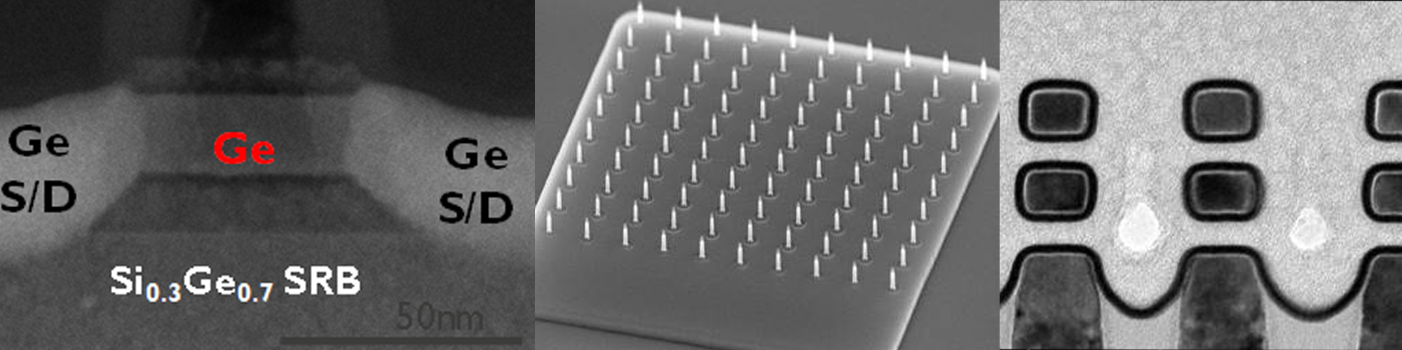
Flexible GeSn Photodetectors Toward Near Infrared Imaging Application
(Nanyang Technological University - Nano Engineering Device Laboratory)
Flexible photonic devices have drawn extensive attention as a promising candidate toward various flexible and wearable applications. Low-cost flexible near infrared (NIR) photodetectors (PDs) have great potential in defense and civilian systems for night-vision applications. Among various materials for flexible PDs, Germanium (Ge) has been one of the most attractive candidates for NIR applications due to its high absorption coefficient, high mobility, and inherent compatibility with CMOS technology. The additional Tin (Sn) and external tensile strain could reduce the bandgap of Ge, leading to efficient transition from indirect to direct band-structure and therefore broader detection wavelength range and higher photo response.
A view on the next generation semiconductor technologies
In this interview, Sri Samavedam, senior vice president CMOS technologies at imec, highlights the major innovations that are needed to advance semiconductor technology development in domains like logic, memory, 3D integration and photonics.
He talks about the various options that imec and its ecosystem of partners are exploring and explains how these can bring value to industry.
Quantum Delta NL Awarded 615 Million Euro From Netherlands’ National Growth Fund To Accelerate Quantum Technology
Monday, April 12, 2021 (Delft, Netherlands): Quantum Delta NL, the public-private foundation, which launched in 2020 with the mandate to coordinate and execute the Netherland’s National Agenda for Quantum Technology (NAQT), today announced that it has been awarded €615 million from the Dutch Ministry of Economic Affairs and Climate Policy to power the advancement of quantum technology.
X-FAB Enters into Collaboration with IHP to Progress SiGe BiCMOS Technology
X-FAB Silicon Foundries and IHP - Leibniz Institute for High Performance Microelectronics have announced a major industry-academic partnership. The objective of the cooperation between these two bodies, which brings together X-FAB’s proficiency in semiconductor manufacture with IHP’s wireless communication expertise, is to exchange knowledge and establish mutually beneficial engineering synergies.
SiPho-G: Advanced GeSi components for next-generation silicon photonics applications
A new European project named SIPHO-G aims to push the boundaries of Ge based stark effect modulator at O- and C- band and avalanche photodiodes to its limits.
See: https://cordis.europa.eu/project/id/101017194
New EU Quantum Flagship consortium launches a project on silicon spin qubits as a platform for large scale quantum computing
GRENOBLE, France – Feb. 4th, 2021 – A European consortium was launched today with the goal of scaling silicon quantum technologies. Named QLSI (Quantum Large-Scale Integration with Silicon), this four-year EU project, coordinated by CEA-Leti, will lay the foundation for the EU's industrial-scale implementation of semiconductor quantum processors and position Europe as a global leader in quantum computing. The project will focus on demonstrating that spin qubits are the leading platform for scaling to very large numbers of quantum bits, or qubits, the building blocks of quantum information processing.
Looking back on imec’s highlights from 2020
2020:
The environmental footprint of logic CMOS technologies
Moving Quantum Computing from Lab to Fab: Imec Presents 300 mm Platform for Silicon Spin Qubit Design
- At the IEEE International Electron Devices Meeting (IEDM2020), imec demonstrates the first flexible hardware platform for silicon spin qubit integration on 300 mm wafers.
- Imec also proposes novel ways to operate multiple qubits in a linear array and to combine classical electronics with quantum circuits at low temperatures.
- These are significant steps forward in the development of large-scale silicon quantum processors, highlighted as a key emerging technology on IEDM.
New materials – new crystal growth equipment
Ultra-pure monoisotopic Silicon/Silicon-Germanium (Si/SiGe) layer stacks are promising candidates for semiconductor-based quantum computer processors. The IKZ initiated Leibniz competition project “SiGeQuant” provides a link from substrate preparing via epitaxial layer growth to quantum bit (qubit) investigating institutions.
Imec presents smallest finFET-based biosensor for high-sensitivity molecule detection
LEUVEN (Belgium), 17 December 2020 — Imec, a world-leading research and innovation hub in nanoelectronics and digital technologies, today presented the smallest silicon finFET that functions as a biosensor. Achieving ultrasmall dimensions (13nm fin width and 50nm gate length), and fabricated with a CMOS-compatible process flow in imec’s 300mm cleanroom, imec envisions volume manufacturing and integration into high-throughput, cost-effective detection tools, with 10,000s of these ‘BioFETs’ working in parallel. With a demonstrated detection limit of tens of molecules today, imec ultimately targets highly accurate BioFETs sensing single DNA molecules.
COMBINING HIGH RESPONSIVITY AND LOW POWER CONSUMPTION IN GRAPHENE-BASED PHOTODETECTORS
Researchers from AMO GmbH, ICFO- Institut de Ciencies Fotoniques, RWTH Aachen University, and Bergishe Universität Wuppertal have developed a novel approach for graphene-based photodetectors that allows combining high responsivity and low power consumption, thus circumventing one of the major limitations of state-of-the-art photodetectors based on graphene – namely the high power-consumption caused by their large dark currents.Read more
Photonics Digital Innovation Hub Lands €19M Investment
BRUSSELS, Oct. 21, 2020 — PhotonHub Europe, a newly established pan-European photonics digital innovation hub, has been awarded a €19 million investment from the European Union’s Horizon 2020 program. The hub will help small- and medium-size enterprises (SMEs) become competitive through accelerated deployment of photonic technologies with the help of a network of experienced institutions, regional photonics hubs, and existing business networks. https://www.photonics.com/Articles/Photonics_Digital_Innovation_Hub_Lands_19M/a66296
High-Quality Crystals for Advanced Research - DESY and Leibniz-Institut für Kristallzüchtung sign cooperation agreement
Cooperation between DESY and the Leibniz-Institut für Kristallzüchtung (IKZ) will literally become closer in the future. The Berlin Leibniz-Institute will establish a branch office on the Hamburg campus. Last week, the two research centers signed a cooperation agreement to this effect, https://www.ikz-berlin.de/en/oeffentlichkeitsarbeit/aktuelles-meldung/high-quality-crystals-for-advanced-research-desy-and-leibniz-institut-fuer-kristallzuechtung-sign-cooperation-agreement
European Capital of Innovation Award 2020
On September 24, 2020, the city of Leuven in Belgium received the European Capital of Innovation 2020 award. The award recognises Leuven’s excellent innovation concepts as well as processes and governance models creating a framework that brings ideas to life. The municipality will receive a €1,000,000 prize funded under Horizon 2020, the EU research and innovation programme. More info on https://ec.europa.eu/info/research-and-innovation/funding/funding-opportunities/prizes/icapital_en
Imec sees five semiconductor trends for the 20s decade
Imec’s CMOS boss Sri Samavedam sees five trends ahead for the semiconductor industry. Read the full article on https://www.electronicsweekly.com/news/business/imec-sees-five-semiconductor-trends-20s-decade-2020-07/.
Imec Demonstrates Excellent Performance of Si FinFET CMOS devices with Integrated Tungsten Buried Power Rails
Lopos, a spin-off of imec and the Ghent University, presents the SafeDistance wearable that helps employees follow social distancing guidelines, https://www.imec-int.com/en/articles/lopos-a-spin-off-of-imec-and-the-ghent-university-presents-the-safedistance-wearable-that-helps-employees-follow-social-distancing-guidelines
Within the framework of a new European H2020 project, nine research institutes and eight industrial partners across the whole value chain are collaborating on innovative solutions to produce silicon photovoltaic (PV) modules with higher performance, lower cost and better environmental profiles compared to commercially available modules. The HighLite project, coordinated by imec, a partner in EnergyVille, aims to substantially improve the competitiveness of the EU PV manufacturing industry by demonstrating new production solutions on pilot-line-level.
New Float-Zone furnace for large silicon crystals (IKZ):
The Float-Zone (FZ) process stands out for its ability to produce volume crystals with ultra-high purity and perfection. The IKZ has acquired a new FZ furnace for the growth of large silicon crystals with a diameter of up to 8 inch (200 mm). This is so far the largest diameter that can be achieved u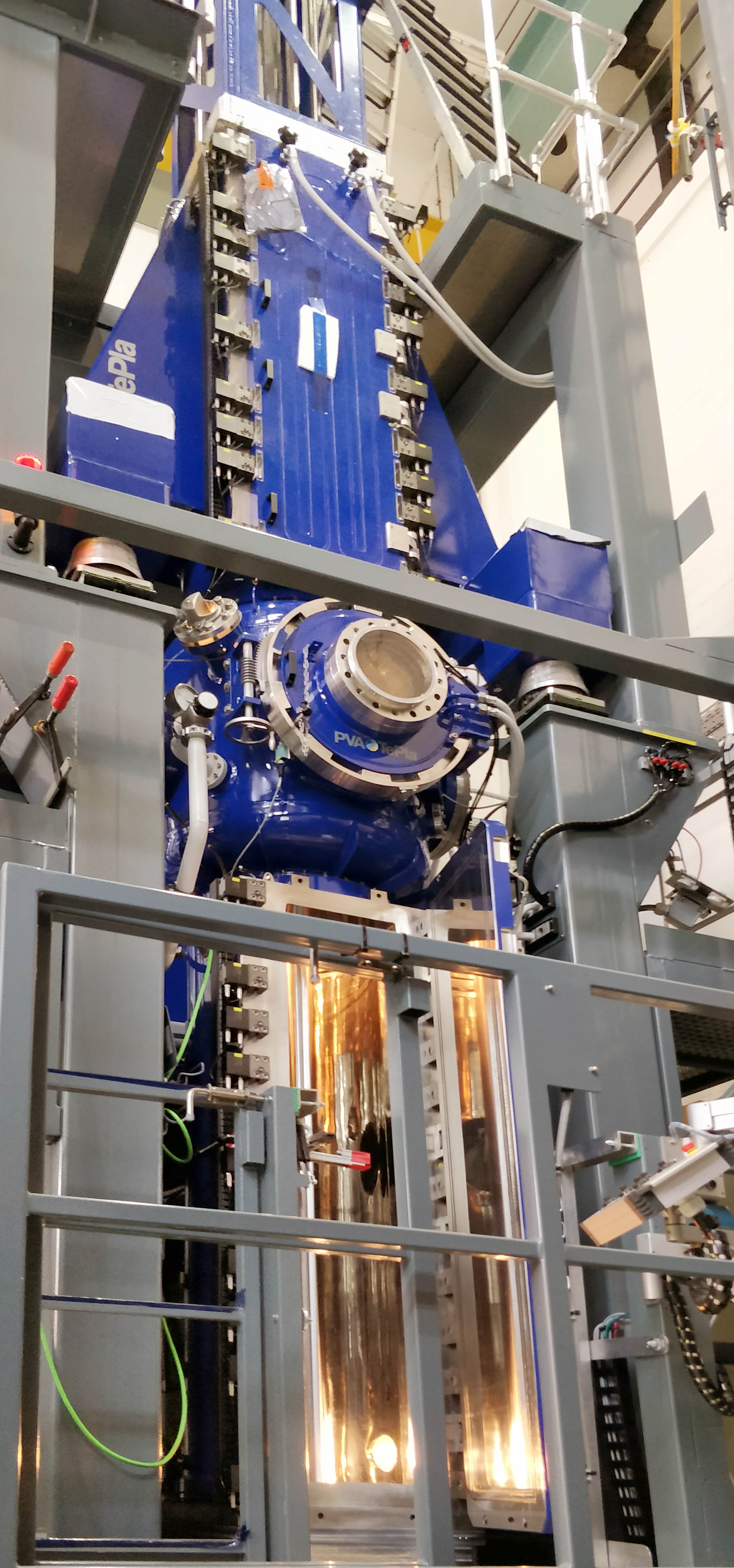 sing the FZ method. With this step the IKZ is able to strengthen its leading role in FZ academic & industrial research.
Size matters – Larger diameter wafers allow for more die per wafer. In the production of high-power semiconductors, with very low content of impurities as oxygen and carbon, the wafer diameter is limited by the FZ process. Power semiconductors (IGBT, MOSFET) are used throughout the entire energy value chain, frm electricity generation, its transmission to its use, e.g. in e-mobility. In consideration of climate change, power semiconductors are gaining in importance as they enable sustainable solutions using intelligent energy management.
The modern crystal growth furnace FZ-30 was funded by the Leibniz-association, in frame of a so called “Sonder-tatbestand“, and built by the company PVA-TePla in Jena, Germany. The technological demands for the furnace with a height of 12 m and a total weight of more than 15 t are challenging. For example, during growth the silicon rods with a weight of more than 100 kg must be moved absolutely vibration-free with millimeter accuracy. In comparison to the three existing FZ furnaces at IKZ, the advanced mechanics of the FZ-30 not only allow the growth of crystals with larger diameter but also at higher process stability and with increased dopant homogeneity in the crystal. The growth chamber withstands an overpressure of the inert gas atmosphere of 3 bar. This reduces the risk of arcing at high heating power of the induction generator with a maximum capacity of 120 KW. With the help of IKZ know-how, the machine type actually designed for industrial production has been extensively modified for research operation, thus extending the available free parameter space for new FZ process development. Additional feedthroughs and process equipment as infrared heaters were added to the growth chamber. The FZ process can be operated via the completely new designed user interface or via the semi-automatic control developed at IKZ.
In the future the FZ-30 will serve for the development of FZ processes, for silicon crystals with higher purity and dopant homogeneity, needed for the next generation of high power semiconductors. For a better controllability of the FZ process especially at large crystal diameter, new automatization concepts will be investigated.
For more info: https://www.ikz-berlin.de/de/aktuell1/news-2/1241-ikz-news-april-2020-neue-fz-anlage
High purity (HP)-Ge crystals have an incredible low impurity level in the range down to <1010 cm-3. This means that only one atom out of 1013 is a foreign atom (ppT level !). Such clean HP-Ge material is needed for Gamma-Ray detector applications in X-Ray Physics, Astronomy etc. IKZ is a member in the international LEGEND project where not natural but even enriched 76Ge detector crystals are needed to make progress on our understanding of the very fundamentals of the Universe.
2019:
IEDM:
-
New Perspectives for Opto-Electronic Platform Technologies (IHP): https://www.ihp-microelectronics.com/en/infocenter/news-center/press-releases/article/new-perspectives-for-opto-electronic-platform-technologies.html
-
Imec shows excellent performance in ultra-scaled FETs with 2D-material channel: https://www.imec-int.com/en/articles/imec-shows-excellent-performance-in-ultra-scaled-fets-with-2d-material-channel
- Imec presents forksheet device as the ultimate solution to push scaling towards the 2nm technology node: https://www.imec-int.com/en/articles/imec-presents-forksheet-device-as-the-ultimate-solution-to-push-scaling-towards-the-2nm-technology-node
Original kilogram replaced - New International System of Units (SI) entered into force on 20 May 2019 (IKZ):
In addition to Ampere, Kelvin, Mol and Co., the kilogram also is now defined by a natural constant. In concrete terms, this means that the original kilogram, which has been the measure of all things for 130 years, has now served its purpose in Paris. This is made possible by the single crystals grown from the highly enriched isotopic silicon-28 at the Leibniz-Institut für Kristallzüchtung (IKZ).
Read the full press release on:
- https://www.fv-berlin.de/en/info-for/the-media-and-public/news/news/ur-kilogramm-abgeloest/
Constructive Multinational Quantum Tech Meeting at IKZ:
Today, quantum technologies gain momentum in research & development for game-changing solutions in the area of computing, communication, sensing, cryptography etc.
The successful realization of quantum technologies depends decisively on atomically engineered crystalline materials with ultra-high precision and here, the expertise of the Leibniz Institut für Kristallzüchtung (IKZ) is worldwide recognized. Specifically, the use of isotope pure Silicon and Germanium (Si/Ge) materials systems is considered a key enabling approach for quantum devices. IKZ substantially benefits in this area of preparing very pure and isotopically enriched Si and Ge crystals from its world leading experience e.g. by metrology projects to define the new kg calibration standard.
On 22nd March 2019, IKZ organized a Si/Ge Quantum Materials workshop to establish the complete value chain from isotopically enriched Si/Ge material purification, single crystal growth as well as heteroepitaxy preparation by CVD and MBE up to manufacturing of Qubit structures, including materials and device characterization on a state-of-the-art level.
For this purpose, IKZ welcomed a group of world leading researchers from Russia (Prof. Petr G. Sennikov, Institute of Chemistry of High-Purity Substances of the Russian Academy of Sciences, Nizhny Novgorod; Prof. Andrey D. Bulanov, Institute of Chemistry of High-Purity Substances of the Russian Academy of Sciences, Nizhny Novgorod; Prof. Alexander A. Ezhevskii, Department of Physics of Semiconductors and Optoelectronics, Nizhny Novgorod Lobachevsky University), from Australia (Prof. Sven Rogge, Department of Condensed Matter Physics, University of New South Wales, Sydney), from Canada (Prof. Oussama Moutanabbir, Department of Engineering Physics, Polytechnique Montréal), from Italy (Prof. Giovanni Capellini, Department of Science, Roma Tre University) and from Germany (Dr. Lars Schreiber, Institute for Quantum Information, RWTH University, Aachen; Dr. Wolfgang Klesse, Leibniz-Institut für innovative Mikroelektronik (IHP), Frankfurt/Oder) to strengthen international links and define solid R & D concepts towards SiGe quantum devices.
IKZ will use its international guest scientist program to strengthen links with these leading research groups by mutual research visits and by initiating common, third party funded research projects.