There are various activities in Graduate School of Engineering, Nagoya University and semiconductor engineering and related materials science are one of the most important research fields in our institute. Research groups in the departments of Materials Physics, Applied Physics, Electrical Engineering, Electronics, Materials Design Innovation Engineering, Materials Process Engineering, and so on are engaged in the semiconductor engineering; materials science, process engineering, device physics, nanostructure analysis, and circuit design, etc. There are also some research centers and consortium related to semiconductor science and technology; Center for Integrated Research of Future Electronics (CIRFE) in Institute of Materials and Systems for Sustainability (IMaSS), Center for Low-temperature Plasma Sciences (cLPS), and GaN consortium.
Following research groups are engaging the research and development for group-IV materials electronics.
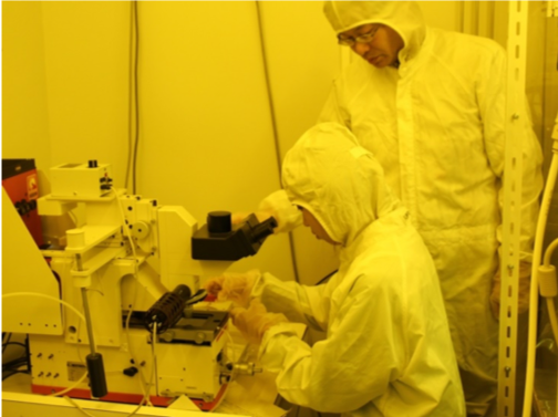
Miyazaki Laboratory (Semiconductor Engineering and Integration Science Laboratory, Research Group of Information Device Engineering, Department of Electronics Engineering)
Link URL http://www.nuee.nagoya-u.ac.jp/labs/miyazakilab/
The continuous downscaling of devices to nanoscale dimensions, following Moore's law, means that silicon based complementary metal-oxide-semiconductor (CMOS) devices, which currently dominate the device industry, are reaching fundamental limits. Our group investigates Si-based semiconductor quantum dots and metal/silicide magnetic nanodots including their process technologies to develop novel functional Si-based devices operating with a few electrons or photons over room temperature. In addition, we also study intensively new generation of nano-electronic devices with new materials and the formation technique for ultra-scaled semiconductor devices with advanced functions. Also, we focus on characterization of electronic defects in dielectrics and at heterostructure interfaces as well as energy band profiles to gain a better understanding of physics for advanced materials and devices.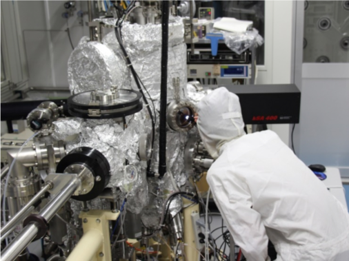
Nakatsuka Laboratory (Nano-Structured Electronic Device Engineering Laboratory, Research Group of Nano-Structured Device Engineering, Department of Materials Physics)
Link URL http://alice.xtal.nagoya-u.ac.jp/nanoeledev/e_index.html
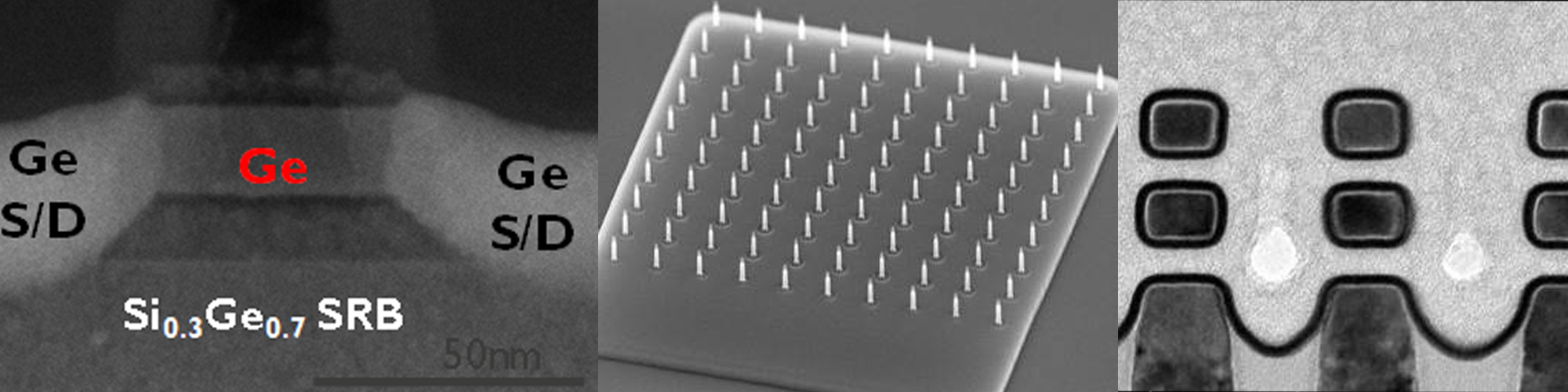
Group-IV family of Si, SiGe, Ge, GeSn, SiGeSn, etc has attracted much attentions for not only nano-electronic devices but also optoelectronics, thermo-electronics, and spintronics applications. These semiconductor materials provides rich energy band designs and noble functions familiar for integrating into Si ULSI technologies. Our group develop and investigate thin-film growth technology of epitaxial and polycrystalline group-IV compound semiconductors on various substrates. Also, we study interface science and technology of metal/semiconductor and metal/oxide/semiconductor structures for integration of these group-IV materials on Si nanoelectronics platform.