Kyushu University
The advanced functional devices division, Global Innovation Center (GIC), Kyushu University focuses on research about group IV semiconductors (Si, Ge)  including their alloy (SiGe, GeSn) and compounds (SiC) process technology and characterization. We promote collaborative study with academic sections and industries all over the world.
Website: https://www.gic.kyushu-u.ac.jp/functionaldevices/index_e.htm
Contacts: Assist Prof. Keisuke YAMAMOTO
Recently we focus on the following topics:
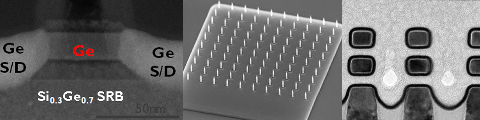
- Ge process technology for MOSFET, optoelectronics, spintronics, and tunnel FET
Ge gate stack
Metal/Ge contact
Ge-on-Insulator
- Polycrystalline Ge, GeSn growth and device fabrication
- Defect characterization in Ge, Ge MOS
- 3C-SiC process technology
Process equipment
Cleanroom (class 1000, 200 m2), ECR sputtering system,
ALD, PVD (sputtering, EB evaporation), electric furnace, RTA, photolithography environment, RIE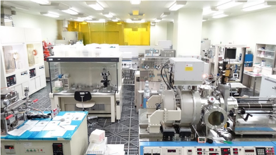
Evaluation equipment
DLTS, Hall effect, C-V/I-V measurements, MOSFET measurements, μ-raman/Photoluminescence, AFM, SEM/TEM (in the same campus), XPS (in the same campus)
Collaborations
Osaka Univ., Japan (Prof. HAMAYA (spintronics))
Tokyo City Univ., Japan (Prof. SAWANO (IV-MBE))
Tsukuba Univ., Japan (Assoc. Prof. TOKO (thin polycrystalline)) Nagoya Univ., Japan (Prof. Nakatsuka)
imec, Belgium
Shanghai Institute of Microsystem and Information Technology, Chinese Academy of Science (Prof. DI)
Recent publications
- K. Yamamoto et al., Fabrication of Ge-on-Insulator By Epitaxial Growth and Ion-Implanted Exfoliation for Electronics and Opt-Electronics Applications, ECS transactions, in press (2021).
- K. Yamamoto et al., Schottky Barrier Height Control at Metal/Ge Interface by Insertion of Nitrogen Contained Amorphous Layer, ECS transactions Vol. 102, No. 4, p. 63 (2021), https://doi.org/10.1149/10204.0063ecst
- H. Nakashima et al., Border-Trap Characterization for Ge Gate Stacks with Thin GeOX layer Using Deep-Level Transient Spectroscopy, ECS transactions, Vol. 98, No. 5, p. 395 (2020), https://doi.org/10.1149/09805.0395ecst
- W.-C. Wen et al., Interface trap and border trap characterization for Al2O3/GeOx/Ge gate stacks and influence of these traps on mobility of Ge p-MOSFET, AIP advances, in press, https://doi.org/10.1063/5.0002100
- R. Oka et al., High interfacial quality metal-oxide-semiconductor capacitor on (111) oriented 3C-SiC with Al2O3 interlayer and its internal charge analysis, Jpn. J. Appl. Phys., Vol. 59, p. SGGD17 (2020), https://doi.org/10.35848/1347-4065/ab6862
- K. Yamamoto et al., Conduction Type Control of Ge-on-Insulator: Combination of Smart-CutTM and Defect Elimination, ECS transactions, Vol. 93, No. 1, p. 73(2019) https://dx.doi.org/10.1149/09301.0073ecst
- K. Moto et al., Polycrystalline thin-film transistors fabricated on high-mobility solid-phase-crystallized Ge on glass, Appl. Phys. Lett., Vol. 114, p. 212107 (2019), https://doi.org/10.1063/1.5093952
- K. Yamamoto et al., Ge field-effect transistor with asymmetric metal source/drain fabricated on Ge-on-Insulator: Schottky tunneling source mode operation and conventional mode operation, Jpn. J. Appl. Phys., Vol. 58, p. SBBA14 (2019), https://doi.org/10.7567/1347-4065/ab02e3
- T. Maekura et al., Fabrication and characterization of asymmetric metal/Ge/metal diodes with Ge-on-Insulator substrate, Jpn. J. Appl. Phys., Vol. 58, p. SBBE05 (2019), https://doi.org/10.7567/1347-4065/aafb5e
- W.-C. Wen et al., Border trap evaluation for SiO2/GeO2/Ge gate stacks using deep-level transient spectroscopy J. Appl. Phys., Vol. 124, Issue 20 p. 205303 (2018), https://doi.org/10.1063/1.5055291
- K. Yamamoto et al., Wide range control of Schottky barrier heights at metal/Ge interfaces with nitrogen-contained amorphous interlayers formed during ZrN sputter deposition, Semiconductor Science and Technology, Vol. 33, p. 114011 (2018), https://doi.org/10.1088/1361-6641/aae4bd