The research activities of the group are focused on the growth of small-sized crystalline materials for devices in the field of energy conversion and electronics. Guidelines are the development of application adequate micro- and nano-crystalline objects and convenient growth methods. The work in the field of group IV elements can be classified within three topics: (1) Growth of polycrystalline Si layers on low-cost substrates, especially on glass. (2) Growth of Si, Ge and SixGe1-x nanowires for thermoelectric and microelectronic applications. (3) Growth of thin tensile strained 28Si layers, cladded by SixGe1-x for quantum computer circuits.
Our research has been and is predominantly financed by third-party funding. It is carried out in cooperation with several international and national partners.
The first topic is focused on the growth of microcrystalline Si layers on amorphous substrates. A specific process, which allows the controlled preparation of seed layers has been developed. Induced by metallic droplets, an amorphous silicon layer deposited by physical vapor deposition is converted into a layer of contiguous microcrystals by an amorphous-liquid-crystalline (ALC) phase transition. Subsequent crystallization of silicon onto the ALC seed layer from a tin solution is achieved at glass compatible temperatures by the temperature difference method (TDM) – a process that has been developed by this team as well. The optimization of this process is supported by numerical modeling of heat and mass transport phenomena using the software CFX. The characterization of structural, optical and electrical properties of the microcrystalline absorber material for solar cells is actually carried out with high priority.
The is embedded in a regional network, in which several doctoral students from different institutions cooperate under the general leadership of the BTU Cottbus/Senftenberg within the framework of the graduate school “Functional Materials and Film Systems for Efficient Energy Conversion” (FuSion). The investigation of the growth of SixGe1-x nanowires (NW) by molecular beam epitaxy (MBE) is an appreciable task of our working group. NWs are very promising for future applications due to the small diameters up to several tenth nanometers. Experiments on Si(001) nano-tip substrates which are provided by the Leibniz-Institut für innovative Mikroelektronik (IHP), Frankfurt (Oder) are especially promising. Vapor-liquid-solid (VLS) grown Ge NW on such Si nano-tips have unique structural features due to the shape forming capability of the liquid gold droplets. On nano-tip substrates Si pillars protrude from an oxidized surface. By varying substrate temperature and gold evaporation rate the exact coincidence of nano-tip density and gold droplet occurrence as precondition for epitaxial growth has been revealed. The alignment into <110> direction is an inherent feature of VLS grown Ge NWs. At the beginning of growth islands with four inclined {111} facets evolve from the nano-tips. Eventually, the gold droplet has to get over to a side facet at some point. Without special arrangement this is an arbitrary process. In this way the starting point and therefore the subsequent nanowire growth within one of the four lateral <110> directions is fixed. The NW growth takes place by strictly straight lateral overgrowth onto the oxide surface. Due to the contact to the substrate plane the common rhombohedral cross section of the NW reduces to the half, i.e. to an isosceles triangle. The lengths of such NW depends solely on growth time. Removing the oxide by wet etching allows the preparation of horizontally free standing Ge bars fixed only at the tips.
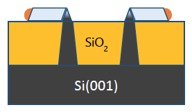
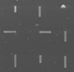
Fig. X: Sketch of the in-plane VLS growth of Ge nanowires on nano-tip Si(001) substrates (left) and top view SEM image of grown Ge nanowires on Si(001) with a tip pitch wide of 1 μm.
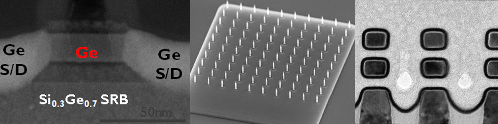
The third topic is promoted by the ongoing Leibniz competition project „High-definition crystalline Silicon-Germanium structures for Quantum circuits“ (SiGeQuant). It will be carried out in cooperation with the Leibniz-Institut für innovative Mikroelektronik (IHP), Frankfurt (Oder), the Institute of Semiconductor Electronics (IHT) of the RWTH Aachen University, and the JARA-Institute for Quantum Information (IQI), an alliance of the 2nd Institute of Physics of the RWTH Aachen university and the Peter-Grünberg Institute at Forschungszentrum Jülich. The IHP provides the so called SiGe virtual substrate. This is a sophisticated layer stack on a convenient Si(100) wafer to realize a dislocation free, atomically flat SiGe surface for epitaxial growth. Our task is the MBE of a tensile strained, nanometre thin layer of monoisotopic 28Si, isomorphic grown in-between SiGe layers. The high-purity 28Si source material for evaporation will be prepared by the IKZ Group-IV (Si & Ge) volume crystals research. The IHT is responsible for the non-invasive configuration of contacts on top of the epitaxial layers. With these contacts the two-dimensional electron gas injected into the 28Si layer will be electrostatically formed within two nearby arranged quantum dots hosting therein single electrons. The IQI will manipulate and evaluate the quantum state of the electrons by electron spin resonance measurements within a 3He/4He dilution refrigerator at 10 mK. This project is intended to develop a CMOS compatible technology for a Si based quantum computer circuit. To be in line with the purity requirements of such a 28Si layer towards electrically active foreign atoms (< 1014 cm-3) and magnetically parasitic 29Si and 73Ge isotopes (~ 1017 cm-3) a one-purpose MBE chamber for the evaporation of small amounts of the expensive 28Si and 72Ge isotopes will be acquired at the end of 2019. All parts of our MBE equipment are designed to process substrates with diameters of up to 100 mm.
Group-IV (Si & Ge) volume crystals research at IKZ, Berlin
Group-IV semiconductors research is one among many key activities of the Leibniz-Institut für Kristallzüchtung (IKZ), Berlin. IKZ is a globally well-known and leading institute in the growth of Si, Ge and SiGe volume (bulk) single crystals for various applications (viz., quantum technology, micro-, nano-, opto-electronics, power devices, etc.). The institute has a unique expertise in growing isotopically pure, perfectly structured single crystals by floating zone (FZ) and Czochralski (Cz) techniques. For example, such grown crystals (28Si) were utilized for the “Avogadro” and “Kilogramm” projects in the redefinition of the fundamental metrology SI unit “mass”. Isotopically pure silicon has lately gained popularity for other applications, e.g. for quantum technologies like quantum computing, sensing etc.. We also have the know-how of growing high-purity (n < 1011 cm-3) Ge single crystals, aimed for “LEGEND” experiments in the area of cosmology. Both of these international projects increased our expertise on isotope pure SiGe crystals and strengthend our international collaboration network.
Czochralski (Si, Ge and their alloys):
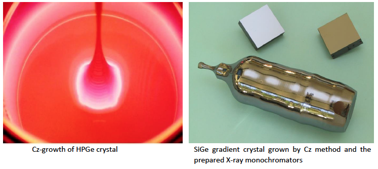
Further focus lies on growing “engineered Si and/or Ge” crystals for the use in: (i) Quantum Computing Technology (isotopic single crystals); (ii) THz Plasmonics (heavily-doped Ge crystals); (iii) Detectors (Ga-doped Ge crystals); (iv) Carrier dynamic studies with Free-Electron-Lasers (Si or Ge crystals specifically doped with Mg, Bi); (v) Synchrotron beam line optics (SiGe mosaic crystals / gradient crystals). It is noted that a number of European
Synchrotron upgrade programs (e.g. the EBS program at the ESRF) set new requests on high performance crystals for accelerator, beamline and experimental facilities.
Float Zone (Si):
Float Zone (FZ) growth of silicon crystals with superior properties is a unique expertise of the Leibniz-Institut für Kristallzüchtung Berlin (IKZ). The FZ lab equipment allows manufacturing of crystals with dimensions ranging from several mm diameter (slim rods) up to large diameter crystals for 6 inch wafers. A new FZ machine capable of growing crystals with a diameter of up to 8 inch is currently brought into operation and will be fully operational in 2020. The ultra-high purity, high resistivity and uniform resistivity distribution achievable in FZ silicon is of paramount importance for electronic applications such as high power devices or in photonics. In addition to the targeted doping with acceptors (e.g. B) and donators (e.g. P), the doping with “exotic” elements such as Bi, Ga, Al, Sb or isoelectric impurity atoms (N, O, C …) is possible. Isotopically pure 28Si FZ crystals have been grown within the scope of the “Avogadro” & “Kilogram” projects that allowed to determine the quantity of the Avogadro constant with unprecedented accuracy in the redefinition of the fundamental metrology SI unit “mass” . A main research focus is the further development of the FZ technology and investigation of underlying crystal growth phenomena. The SiGrEt project aims to prove the feasibility of a novel FZ-like growth concept, which may allow cost efficient growth of crystals with a high quality at the level of FZ silicon. For FZ process optimization, a 3D time-dependent numerical model was developed in collaboration with international industry partners. For advanced FZ process automatization, a model-predictive control system was developed. Research activities are accompanied by making use of a wide range of characterization methods, such as the Lateral Photovoltage Scanning (LPS) method, which was developed at IKZ for photoelectric crystal diagnostics and is in great demand by our worldwide partners.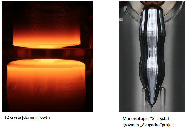
For more details visit our web page: www.ikz-berlin.de