![]()
Light emission from SiGe
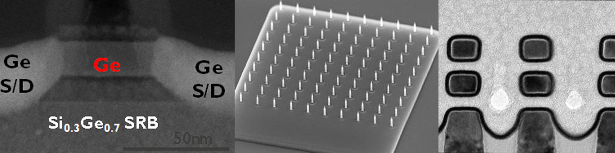
Our research aims to revolutionize the electronics industry by adding intra-chip and chip-to-chip communication at the speed of light, offering significantly reduced energy consumption. Cubic crystal phase SiGe is known to be great for electronics. We propose to develop hexagonal crystal phase SiGe (Hex-SiGe), which features a direct bandgap and will add photonic capabilities to electronics. Direct bandgap silicon has been the holy grail of the semiconductor industry for many years, since it would allow integrating both electronic and optical functionalities on a silicon platform. Recent theoretical calculations predict that hexagonal crystal phase SixGe1-x features a tunable direct bandgap from 1380-1800 nm, exactly coinciding with the low loss window for optical fibre communications. We have recently developed a generic approach to grow defect-free hexagonal SixGe1-x with tunable composition. Aim is to demonstrate efficient light emission from direct bandgap SiGe, followed by the development of a SiGe nanolaser.
1. E. M.T. Fadaly et al. Direct Bandgap Emission from Hexagonal Ge and SiGe Alloys. https://arxiv.org/abs/1911.00726
2. S. Assali et al., Strain engineering in Ge/GeSn core/shell nanowires, APPLIED PHYSICS LETTERS. Volume: 115 , Issue: 11, Article Number: 113102 (2019), DOI: 10.1063/1.5111872
3. Hexagonal silicon grown from higher order silanes. By: Ren, Yizhen; Leubner, Philipp; Verheijen, Marcel A.; et al. NANOTECHNOLOGY Volume: 30 Issue: 29 Article Number: 295602 Published: JUL 19 2019 DOI: 10.1088/1361-6528/ab0d46
4. Critical strain for Sn incorporation into spontaneously graded Ge/GeSn core/shell nanowires. By: Albani, Marco; Assali, Simone; Verheijen, Marcel A.; et al. NANOSCALE Volume: 10 Issue: 15 Pages: 7250-7256 Published: APR 21 2018, DOI: 10.1039/c7nr09568f
5. Optical Emission in Hexagonal SiGe Nanowires. By: Cartoixa, Xavier; Palummo, Maurizia; Hauge, Hakon Ikaros T.; et al. NANO LETTERS Volume: 17 Issue: 8 Pages: 4753-4758 Published: AUG 2017, DOI: 10.1021/acs.nanolett.7b01441
6. Growth and Optical Properties of Direct Band Gap Ge/Ge0.87Sn0.13 Core/Shell Nanowire Arrays. By: Assali, S.; Dijkstra, A.; Li, A.; et al. NANO LETTERS Volume: 17 Issue: 3 Pages: 1538-1544 Published: MAR 2017, DOI: 10.1021/acs.nanolett.6b04627
7. Single-Crystalline Hexagonal Silicon-Germanium. By: Hauge, Hakon Ikaros T.; Conesa-Boj, Sonia; Verheijen, Marcel A.; et al. NANO LETTERS Volume: 17 Issue: 1 Pages: 85-90 Published: JAN 2017, DOI: 10.1021/acs.nanolett.6b03488
8. Hexagonal Silicon Realized. By: Hauge, Hakon Ikaros T.; Verheijen, Marcel A.; Conesa-Boj, Sonia; et al. NANO LETTERS Volume: 15 Issue: 9 Pages: 5855-5860 Published: SEP 2015, DOI: 10.1021/acs.nanolett.5b01939
Ge/Si Quantum Materials
we synthesize materials and nanoscale devices which exhibit unconventional quantum-physical effects. We focus on heavy-element semiconductors like InSb and PbTe, as they feature large spin-orbit couplings and small effective masses, and on Ge/Si core/shell nanowires, in which the lattice strain is expected to result in high spin-orbit energies. Given their spatial confinement in two dimensions, nanowires of these types of materials are ideal candidates for experiments which rely on low-dimensional effects. To grow nanowires, we use state-of-the-art metal-organic-vapour-phase epitaxy and molecular-beam epitaxy. We put great effort into maximizing the crystalline quality, purity and structural complexity of our materials and devices.
1. J. Ridderbos et al. Hard Superconducting Gap and Diffusion-Induced Superconductors in Ge-Si Nanowires, NANO LETTERS, Volume: 20 Issue: 1 Pages: 122-130 (2019) , DOI: 10.1021/acs.nanolett.9b03438
2. Multiple Andreev reflections and Shapiro steps in a Ge-Si nanowire Josephson junction. By: Ridderbos, Joost; Brauns, Matthias; Li, Ang; et al. PHYSICAL REVIEW MATERIALS Volume: 3 Issue: 8 Article Number: 084803 Published: AUG 14 2019, DOI: 10.1103/PhysRevMaterials.3.084803
3. Josephson Effect in a Few-Hole Quantum Dot. By: Ridderbos, Joost; Brauns, Matthias; Shen, Jie; et al. ADVANCED MATERIALS Volume: 30 Issue: 44 Article Number: 1802257 Published: NOV 2 2018, DOI: 10.1002/adma.201802257
4. Spin-Orbit Interaction and Induced Superconductivity in a One-Dimensional Hole Gas. By: de Vries, Folkert K.; Shen, Jie; Skolasinski, Rafal J.; et al. NANO LETTERS Volume: 18 Issue: 10 Pages: 6483-6488 Published: OCT 2018, DOI: 10.1021/acs.nanolett.8b02981
5. Single, double, and triple quantum dots in Ge/Si nanowires. By: Froning, F. N. M.; Rehmann, M. K.; Ridderbos, J.; et al. APPLIED PHYSICS LETTERS Volume: 113 Issue: 7 Article Number: 073102 Published: AUG 13 2018, DOI: 10.1063/1.5042501
6. Boosting Hole Mobility in Coherently Strained [110]-Oriented Ge-Si Core-Shell Nanowires. By: Conesa-Boj, S.; Li, A.; Koelling, S.; et al.NANO LETTERS Volume: 17 Issue: 4 Pages: 2259-2264 Published: APR 2017, DOI: 10.1021/acs.nanolett.6b04891
7. Highly tuneable hole quantum dots in Ge-Si core-shell nanowires. By: Brauns, Matthias; Ridderbos, Joost; Li, Ang; et al. APPLIED PHYSICS LETTERS Volume: 109 Issue: 14 Article Number: 143113 Published: OCT 3 2016, DOI: 10.1063/1.4963715
8. Electric-field dependent g-factor anisotropy in Ge-Si core-shell nanowire quantum dots. By: Brauns, Matthias; Ridderbos, Joost; Li, Ang; et al. PHYSICAL REVIEW B Volume: 93 Issue: 12 Article Number: 121408 Published: MAR 17 2016, DOI: 10.1103/PhysRevB.93.121408