Experimental Physics and Functional Materials
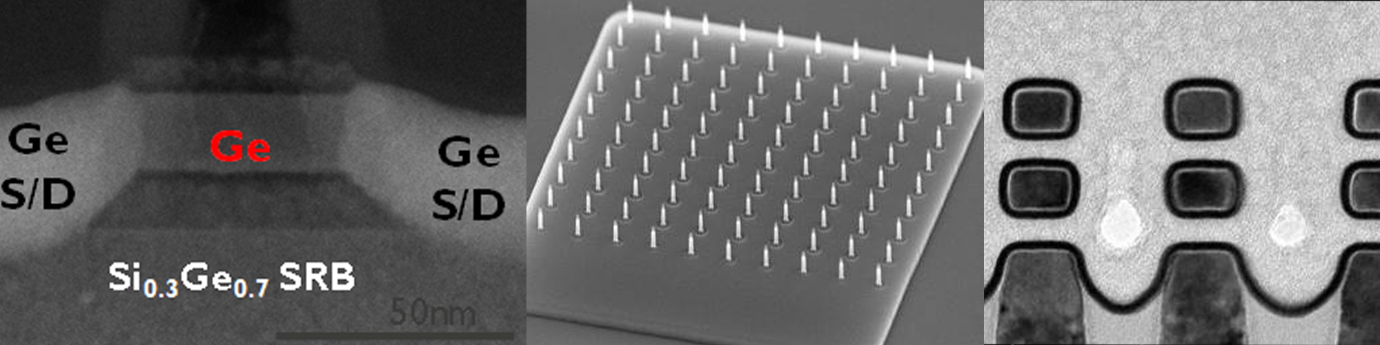
Our research is aimed at the development, fabrication and characterization of nano- and optoelectronic devices based on the group-IV semiconductors Silicon, Germanium and Tin. We combine materials research with the development of novel device concepts with applications ranging from integrated photonics to sensing. One example is the use of low-dimensional semiconductor heterostructures and metallic nanostructures to develop integrated biosensors. We are one of the 12 Microelectronics Research Labs in Germany that receive funding by the Federal Ministry for Education and Research (BMBF) for state-of-the-art equipment used for research on innovative materials and devices.
https://www.b-tu.de/en/fg-exphysik-funktionale-materialien
- Materials research: Our research on group-IV semiconductor alloys is focused on the fabrication and characterization of semiconductor nanostructures such as quantum wells and quantum islands:
• https://aip.scitation.org/doi/abs/10.1063/1.4953784
• https://journals.aps.org/prmaterials/abstract/10.1103/PhysRevMaterials.4.024601
- Optoelectronic devices: The semiconductor alloy GeSn is a direct semiconductor at high Sn content (in contrast to Ge) and, thus, ideally suited for application in optoelectronic components. Our research on the combination of metallic nanostructures (plasmonics) with optoelectronic devices (photonics) has potential applications that range from on-chip biosensing to quantum information processing:
• https://pubs.acs.org/doi/abs/10.1021/acsphotonics.8b01067
• link.springer.com/article/10.1007/s10404-017-2007-3