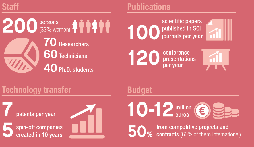
Short description of activities
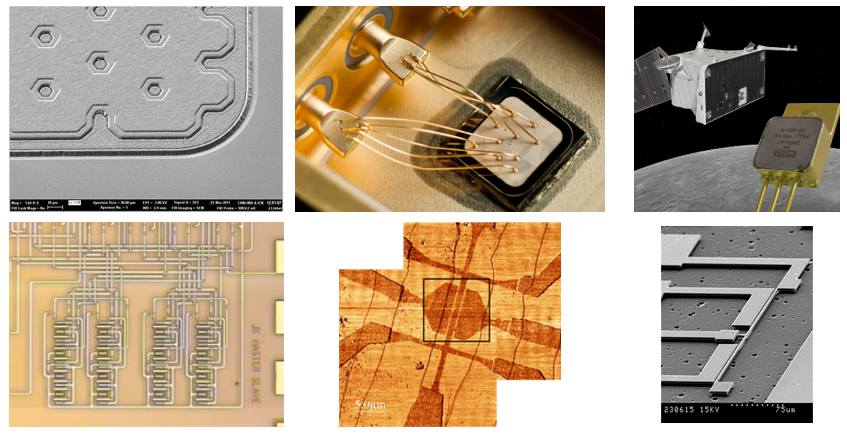
The research activities within Group IV semiconductors mainly concentrate on process technology optimization for reliable silicon, silicon carbide (SiC) and Carbone based devices. The devices are fabricated in our IMB-CNM Clean Room and they are intended for various application fields (energy, mobility, high frequency, harsh environment, space applications, high energy physics experiments, etc.). The research studies cover the simulation, design, fabrication and characterization of a wide range of structures (Schottky diodes, bipolar diodes, MOS capacitances, MESFETs, MOSFETs, JFETs, etc…), as well as their integration in basic ICs.
1. Optimized process technologies for wide bandgap semiconductors: silicon carbide (SiC), gallium nitride on silicon (GaN on Si) and more recently diamond.
Some of the main issues addressed in SiC and GaN technology cover from junction and contact formation to optimization of gate oxidation process, with research on different approaches to improve the gate dielectric and its interface with the semiconductor (Rapid Thermal Processing, TEOS PECVD, nitridation, high-k dielectrics, etc…), as well as other treatments, like boron-doped gate dielectrics for high channel mobility SiC MOSFETs.
An important part of the activities concentrates also on dedicated electrical characterization and reliability assessment techniques of the involved WBG technologies, including for example characterization at different temperatures, bias-stress instability and radiation hardness stability studies.
2. Fabrication of high-temperature devices (diodes, sensors, integrated circuits) for aeronautical and space applications.
Taking profit of the available advanced technology, SiC devices for sensors applications (Hall sensors, Gas sensors, UV detectors, Biomedical sensors, NEMS, etc...) are also a matter of research, some of them in collaboration with other multidisciplinary Groups. We have also developed digital electronic gates and basic circuits like flip-flop for high temperature (300ºC) integrated circuits. We are currently working on high temperature SiC CMOS structures, as well as on the development of wide temperature range (-40ºC-300ºC) voltage references.
3. Study of carbon-based materials
Another relevant activity is toward the study and technology integration of carbon-based materials as, for example, epitaxial graphene on SiC or CVD graphene, carbon nanotubes and, more recently, diamond devices. Processing technologies for the implementation of Carbone based devices are under development and several devices demonstrators have been successfully obtained. Applications in different fields like quantum technology, metrology, biosensors are contemplated.
These activities have been developed in the framework of different National and International Research Projects and Industrial contracts, as for example:
• Green Electronics with Diamond Power Devices (GreenDiamond), H2020-LCE-2014-1, Grant agreement ID: 640947, May 2015 – Apr. 2020
• Silicon Carbide Power Technology for Energy Efficient Devices (SPEED), FP7-NMP-2013-LARGE-7, Grant agreement ID: 604057, Jan. 2014 - Dec. 2018
• Current Limiting Device to Address DC Aeronautics Power Distribution Systems (FUSES 2014), SP1-JTI-CS-2013-03, Grant agreement ID: 641336, 1 Sep 2014 – 31 Aug 2016
• Prototyping and characterisation of radiation hardness of SiC MOS structures
European Space Agency: 01ITT AO/16962/12/NL/SFe, 1 july 2015 – 31 may 2018
• Training NETwork on Functional Interfaces for SiC (NETFISIC), FP7-PEOPLE-2010-ITN, Grant agreement ID: 264613, 1 Feb 2011 – 31 Jan 2015
• Development of a high voltage Silicon Carbide (SiC) normally–on JFET with vertical conduction architecture for cascode applications
Industrial contract with Monolithic Power Systems (US) 01/06/2018 - 31/09/2020
• Fabrication of epitaxial graphene on silicon carbide
Industrial contract with Graphene Nanotech (Spain
For more details, please visit our web page: http://www.imb-cnm.csic.es/index.php/en/
Contact:
|
Prof. Philippe Godignon |
Email: This email address is being protected from spambots. You need JavaScript enabled to view it. |
|
Dr. Joan Marc Rafí |
Email: This email address is being protected from spambots. You need JavaScript enabled to view it. |
Selected representative publications (2015-2020)
2020:
J.M. Rafí, G. Pellegrini, P. Godignon, et al., Electron, neutron and proton irradiation effects on SiC radiation detectors, IEEE Transactions on Nuclear Science 67 (12), 2481-2489 (2020), https://doi.org/10.1109/TNS.2020.3029730
M.C. Jiménez-Ramos, et al., IBIC analysis of SiC detectors developed for fusion applications, Radiation Physics and Chemistry 177, 109100 (2020), https://doi.org/10.1016/j.radphyschem.2020.109100
J.C. Hönig, et al., Investigation of nitrogen enriched silicon for particle detectors, Journal of Instrumentation 15, P05006 (2020), https://doi.org/10.1088/1748-0221/15/05/P05006
S. Aslanidou, A.García-García, P. Godignon, G. Rius, Electronic interface and charge carrier density in epitaxial graphene on silicon carbide. A review on metal–graphene contacts and electrical gating, APL Materials 8, 100702 (2020), https://doi.org/10.1063/5.0022341
2019:
M. Cabello, et al., Comparative study of boron doped gate oxide impact on 4H and 6H-SiC n-MOSFETs, Materials Science in Semiconductor Processing 93, 357-359 (2019), https://www.sciencedirect.com/science/article/pii/S1369800118319309
E. Masvidal-Codina, et al., High-resolution mapping of infraslow cortical brain activity enabled by graphene microtransistors, Nature Materials 18, 280-299 (2019), https://www.nature.com/articles/s41563-018-0249-4
V. Banu, M. Popescu, P. Godignon, Delta Reference, the Latest High Temperature Compensated Voltage Reference Concept, European Space Power Conference (ESPC) Juan-les-Pins, FRANCE SEP 30-OCT 04, 2019
2018:
V. Soler, M. Cabello, V. Banu, J. Montserrat, J. Rebollo and P. Godignon, Complementary p-Channel and n-Channel SiC MOSFETs for CMOS Integration, Material Science Forum, vol. 924, pp.975-979 (2018)
O. Loto, et al., Gate Oxide Electrical Stability of p-type Diamond MOS Capacitors, IEEE Transactions on Electron Devices 65, 3361-3364 (2018), https://ieeexplore.ieee.org/document/8399540
M. Cabello, et al., Advanced processing for mobility improvement in 4H-SiC MOSFETs: A review, Materials Science in Semiconductor Processing 78, 22-31 (2018), https://www.sciencedirect.com/science/article/pii/S1369800117318978
F. Roccaforte and P. Godignon, Wide band gap semiconductors technology for next generation of energy efficient power electronics, Editorial of Special Issue Materials Science in Semiconductor Processing 78, 1-1 (2018), https://www.sciencedirect.com/science/article/pii/S136980011830101X
C. Hebert, et al., Flexible Graphene Solution-Gated Field-Effect Transistors: Efficient Transducers for Micro-Electrocorticography, Advanced Functional Materials 28, 1703976, (2018), https://onlinelibrary.wiley.com/doi/full/10.1002/adfm.201703976
J.M. Rafí, et al., Four-quadrant silicon and silicon carbide photodiodes for beam position monitor applications: electrical characterization and electron irradiation effects, Journal of Instrumentation 13, C01045, (2018), https://iopscience.iop.org/article/10.1088/1748-0221/13/01/C01045
2017:
V. Soler, et al., High-Voltage 4H-SiC Power MOSFETs With Boron-Doped Gate Oxide, IEEE Transactions on Industrial Electronics 64, 8962-8970 (2017), https://ieeexplore.ieee.org/document/7968463
J.C. Pinero, et al., Impact of Thermal Treatments in Crystalline Reconstruction and Electrical Properties of Diamond Ohmic Contacts Created by Boron Ion Implantation, Physica Status Solidi A 214, 1700230 (2017), https://onlinelibrary.wiley.com/doi/full/10.1002/pssa.201700230
M. Cabello, et al., Impact of boron diffusion on oxynitrided gate oxides in 4H-SiC metal-oxide-semiconductor field-effect transistors, Applied Physics Letters 111, 042104 (2017), https://aip.scitation.org/doi/10.1063/1.4996365
2016:
V. Banu, et al., Power cycling analysis method for high-voltage SiC diodes, Microelectronics Reliability 64, 429-433 (2016), https://www.sciencedirect.com/science/article/pii/S0026271416301913
2015:
M. Alexandru, et al., SiC Integrated Circuit Control Electronics for High-Temperature Operation, IEEE Transactions on Industrial Electronics 62, 3182-3191 (2015), https://ieeexplore.ieee.org/document/6982217
J. Leon, et al., Local non invasive study of SiC diodes with abnormal electrical behavior, Solid-State Electronics 113, 35-41 (2015), https://www.sciencedirect.com/science/article/pii/S0038110115001409
T. Phulpin, et al., Failure analysis of ESD-stressed SiC MESFET, Microelectronics Reliability 55, 1542-1548 (2015), https://www.sciencedirect.com/science/article/pii/S0026271415300585
G. Pristavu, et al., A model to non-uniform Ni Schottky contact on SiC annealed at elevated temperatures, Applied Physics Letters 106, 261605 (2015), https://aip.scitation.org/doi/10.1063/1.4923468
V. Banu, P. Godignon, J. Millan, Design of Voltage Comparator Integrated Circuit with Normally-On MESFETs on 4H-SiC semiconductor, IEEE International Semiconductor Conference Sinaia (Romania) OCT 12-14, 2015
Short description of IMB-CNM-CSIC
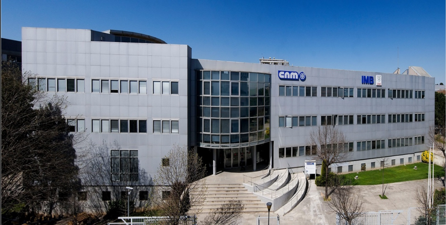
The Institute of Microelectronics of Barcelona (IMB-CNM) is the largest institute in Spain dedicated to the research and development of Micro and Nano Technology (MNTs) and microsystems and the unique with the capacities of silicon technology in Spain. It belongs to the Spanish National Research Council (CSIC) since its foundation in 1985
IMB-CNM is located in Bellaterra (Cerdanyola del Vallès), on the Campus of the Autonomous University of Barcelona (UAB), which is a privileged environment for both basic and applied/industrial research. It is a member of the Barcelona Nanotecnology Cluster-Bellaterra. The IMB-CNM as part of CSIC is also a member of the UAB Research Parc (PRUAB).
IMB-CNM mission is to perform applied research based on micro and nanotechnologies, mainly focused towards the development of components and micro and nano systems. IMB-CNM aims to contribute to the advancement of knowledge and to the economic and social development of society, as well as to the training of researchers and engineers and to the advice to public and private entities.
Intelligent miniaturized systems, eventually with integrated electronic, photonic, mechanical components and circuits, play an important role in society. Research, development and application of miniaturized components and systems will improve the health and well-being of people, help control environmental conditions, save and improve efficient management of energy. IMB-CNM aims to be a recognized contributor in exploring and developing micro and nanotechnologies for the realization of miniaturized components and systems. Its experience in micro and nanotechnologies enables IMB-CNM to lead projects ranging from academic research to industrial contracts, in an international environment.
The R&D activities of IMB-CNM are complemented with training of students, researchers and engineers and with technology transfer to companies.
IMB-CNM also participates in Spanish and International Technology Platforms and Networks of Excellence and has established collaborative agreements with various universities and research centres, to which it offers cooperation in their R&D activities and also access to manufacturing technologies through the "Integrated Micro and Nanofabrication Clean Room". This infrastructure has been recognized by the Ministry of Economy and Competitiveness with the National label of large-scale infrastructure (Instalación Científica y Tecnológica Singular - ICTS).

IMB-CNM summary